1. Ceramic packaging: In ceramic packaging, a metal paste printed circuit board is usually used as the bonding area and the capping area. Before the surface of these materials are electroplated with nickel and gold, the use of Guoxing plasma cleaning can remove organic pollutants and significantly improve the quality of the coating. 2. Surface treatment of the lead frame: The plastic packaging form of the lead frame is still the mainstream in the field of microelectronic packaging. The lead frame is mainly made of copper alloy materials with good thermal conductivity, electrical conductivity and good processing properties. Copper oxides and other organic contaminants can cause delamination between the sealing mold and the copper lead frame, leading to poor sealing performance and chronic air leakage after packaging. At the same time, it will also affect the quality of chip bonding and wire bonding, and ensure the ultra-cleanness of the lead frame. The key to ensuring packaging reliability and yield. Guoxing technology plasma treatment can achieve the effect of ultra-purification and activation of the lead frame surface. Compared with traditional wet cleaning, the yield rate is greatly improved. 3. Pre-treatment of chip bonding: The bonding between the chip and the package substrate is often two materials with different properties. The surface of this material is usually hydrophobic and inert, and its surface bonding performance is poor, and interfaces are prone to appear during the bonding process. The generation of voids brings great safety hazards to the packaged chips. Plasma treatment on the surface of the chip and the package substrate can effectively improve the surface activity and greatly improve the fluidity of the surface bonding epoxy resin. Improve the bonding and wettability of the chip and the package substrate, reduce the delamination between the chip and the substrate, improve the thermal conductivity, improve the reliability and stability of the IC package, and increase the service life of the product. In terms of flip chip packaging, plasma treatment of the chip and the package carrier can not only get an ultra-clean soldering surface, but also greatly improve the activity of the soldering surface, which can effectively prevent false soldering, reduce voids, and improve soldering reliability. Increase the edge height and the tolerance of the filler, improve the mechanical strength of the packaging, reduce the internal shear force formed between the interface due to the thermal expansion coefficient of different materials, and improve the reliability and service life of the product. 4. Wire bonding: The quality of integrated circuit wire bonding has a decisive influence on the reliability of microelectronic devices. The bonding area must be free of contaminants and have good bonding properties. The presence of contaminants such as oxides and organic residues will severely weaken the pull value of the wire bond. Traditional wet cleaning cannot completely remove or cannot remove contaminants in the bonding area. Plasma cleaning can effectively remove the surface contamination of the bonding area, activate the surface, and significantly increase the bonding tension of the wire. Greatly improve the reliability of packaging equipment
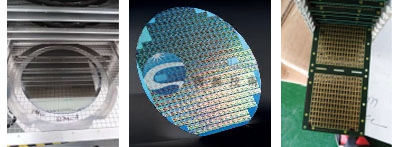
Semiconductor cleaning application case pictures


Consult now